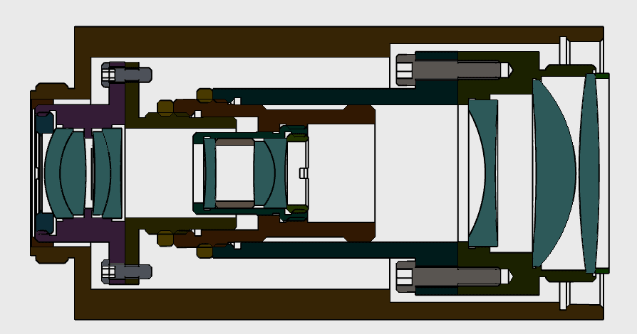
Our expertise in the design and manufacture of precision optics and optical imaging subsystems originates from our engineering team’s extensive experience in the design and manufacture of complex small and large microscope objectives and lens assemblies, as well as large precision optics for wafer inspection equipment. With many decades of collective experience in the design, assembly and test of complex optomechanical lens assemblies, JML is a trusted partner to the semiconductor industry.
Cutting-Edge Semiconductor Optics for Next-Generation Semiconductor Devices
As semiconductor manufacturing technology stays up-to-date with new developments in semiconductor chip architecture—where the trend is the continued decrease in feature size, yet increase in design complexity—one constant is the demand for cutting-edge inspection tools that accurately and precisely inspect wafers at high throughput, repeatedly and reliably. These tools require precision, custom optics, and optical assemblies (e.g., microscope objectives) that produce high-resolution images across a large field of view (FOV) in a variety of different modalities and be designed to work with LED or laser illumination and used in conjunction with precision motion control systems.
Expertise & Experience
At JML, we engage with our customers to design and deliver custom spherical, aspheric, and cylindrical optics and optical assemblies that enable high-resolution imaging and superior data collection in state-of-the-art wafer inspection and metrology systems inspection operating over 400nm to 2.4μm in dark/bright field, fluorescence, photoluminescence and other detection. Our collaborative partnership model helps accelerate product and process development, keeping time-critical projects on schedule and on budget to enable our customers to be first-to-market with industry-leading solutions.
We are a Proven Supplier of Semiconductor Optics for:
- Wafer inspection tools
- Interferometric topography inspection
- Defect mapping systems (white/dark field, photoluminescence, NIR)
- Flat panel display measurement tools
Examples of JML’s Impact in Semiconductor Industry:
- Custom high-resolution microscope objectives operating in 400nm to 2.4μm
- Optomechanical subsystems
- Large optical assemblies; 350mm diameter spherical optics for wafer inspection
- Precision cylindrical lenses for line generation for high-throughput inspection tools

